
When DeepMind’s AlphaGo defeated Go world champion Lee Sedol in March 2016, it showcased a landmark moment in artificial intelligence. This match utilized hardware Google had operated in production for over a year without public acknowledgment. The Tensor Processing Unit, or TPU, embodied a significant shift in computing methodology, emphasizing that sometimes doing less achieves more.
Since 2015, Google’s TPU family has advanced through seven generations, scaling from single-chip processing of image recognition queries to 9,216-chip supercomputers training the largest language models existing today. This article explores why Google developed custom silicon and explains its function, highlighting the physical limitations and engineering trade-offs involved.
In 2013, Google’s infrastructure team conducted an analysis revealing that if Android users adopted voice search as projected—using it for only three minutes daily—the computational demand would necessitate doubling the company’s entire global data center footprint. At that time, expanding with traditional processors was economically unfeasible. More importantly, Moore’s Law, which predicted transistor density doubling approximately every two years, had been slowing. Waiting for the next generation of CPUs from Intel was not a viable option.
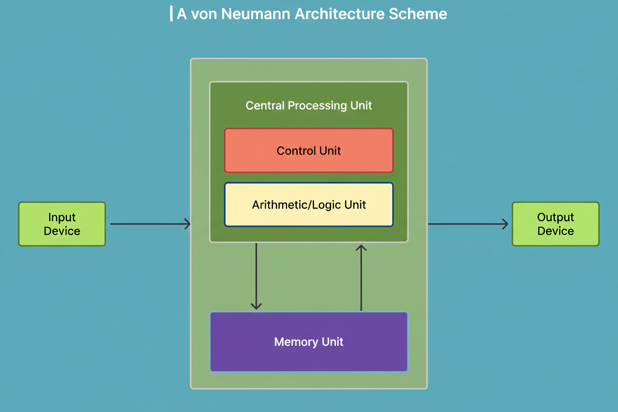
The fundamental issue was architectural. Conventional computers follow the Von Neumann architecture, where the processor and memory communicate over a shared bus. Each calculation involves fetching instructions, retrieving data from memory, executing operations, and writing results back. This creates the Von Neumann bottleneck, where the energy cost of data movement can exceed that of computation itself.
To illustrate, consider a chef who must repeatedly walk to a distant pantry for each ingredient—the cooking might take seconds, but the walking takes hours. Such design makes sense for general-purpose tasks like word processing or browsing because workloads are unpredictable. However, neural networks differ fundamentally.
Deep learning models primarily execute matrix multiplication. They multiply input data by weight matrices, add bias, and apply activation functions billions of times per prediction. Large language models with hundreds of billions of parameters demand hundreds of billions of multiply-add operations per query. These operations are predictable, parallel, and deterministic.
CPUs expend considerable processing power on features like branch prediction and out-of-order execution designed for unpredictable code. GPUs improved performance with thousands of cores but retained architectural overhead from their graphics origins. Google’s approach was to create silicon dedicated solely to neural networks’ needs, stripping away unnecessary functions.
The TPU’s core architecture is the systolic array, named after the rhythmic heartbeat-like data pulsing through the chip. Different processors handle tasks distinctively:
Within the TPU, the workers are multiply-accumulate units arranged in a dense 256 by 256 grid for the first generation, totaling 65,536 calculators operating simultaneously. Computation proceeds as:
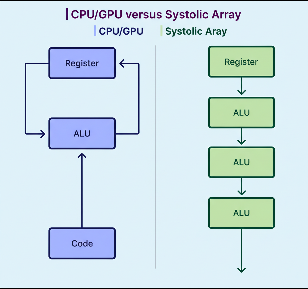
This design reads data from memory once but reuses it thousands of times while traversing the array, eliminating the traditional processor’s memory-access bottleneck. Data moves only between physically adjacent calculators via short wires, sharply reducing energy consumption.
Performance metrics validate this approach. TPU v1’s 256 by 256 array delivered 65,536 multiply-accumulate operations per clock cycle. Operating at 700 MHz, it achieved 92 trillion 8-bit operations per second while consuming just 40 watts. Contemporary GPUs perform tens of thousands of operations per cycle, whereas TPU executes hundreds of thousands.
More than 90% of the TPU’s silicon performed useful computation, compared to approximately 30% in GPUs. This specialization restricts TPU ability to matrix multiplication exclusively, making it unsuitable for general tasks like graphics or web browsing. However, Google embraced this constraint since neural network inference is predominantly matrix multiplication repeated extensively.
The systolic array depends on carefully orchestrated supporting components to optimize end-to-end performance, addressing bottlenecks from raw data to AI predictions.
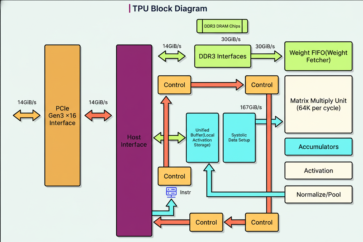
Key components include:
The Matrix Multiply Unit (MXU) constitutes the systolic array. TPU v1 utilized a single 256-by-256 array processing 8-bit integers. Subsequent versions adopted 128-by-128 arrays with Google’s BFloat16 format for training workloads, before returning to 256-by-256 arrays in v6 to quadruple throughput. The weight-stationary design minimizes energy-consuming data movement.
The Unified Buffer features 24 megabytes of on-chip SRAM, acting as a high-speed staging area bridging slower external memory and the MXU’s high demand. It stores input activations, intermediate outputs between neural network layers, and final results prior to dispatch. Being on-chip, this memory has considerably higher bandwidth than external memory, ensuring continuous data supply to the MXU without idle waiting.
The Vector Processing Unit (VPU) handles computations that exceed the MXU’s scope, such as activation functions including ReLU, sigmoid, and tanh. These nonlinear functions enable networks to learn complex patterns; without them, multiple layers collapse into a single linear transformation. Dedicated hardware circuits compute activations in a single cycle. Data typically flows from MXU to VPU before progressing to subsequent network layers.
Accumulators gather 32-bit results output from the MXU. When multiplying 8-bit inputs, products yield 16-bit values, but repeated additions increase sum size. Using 32-bit accumulators prevents overflow during matrix multiplications requiring multiple additions. Accumulator memory totals 4 megabytes spread across 4,096 vectors of 256 elements each.
The Weight FIFO buffer facilitates weight staging between external memory and the MXU employing double-buffering. The MXU maintains two sets of weight tiles: one actively computing, while the other loads from memory. This overlap completely hides memory latency, preventing the computation units from waiting on data.
High Bandwidth Memory (HBM) technology evolved significantly across TPU generations. The original TPU v1 utilized DDR3 memory delivering 34 gigabytes per second bandwidth. Modern TPU Ironwood achieves 7.4 terabytes per second, a 217-fold improvement. HBM stacks multiple DRAM dies vertically interconnected with thousands of connections, enabling bandwidth impossible with traditional memory packaging.
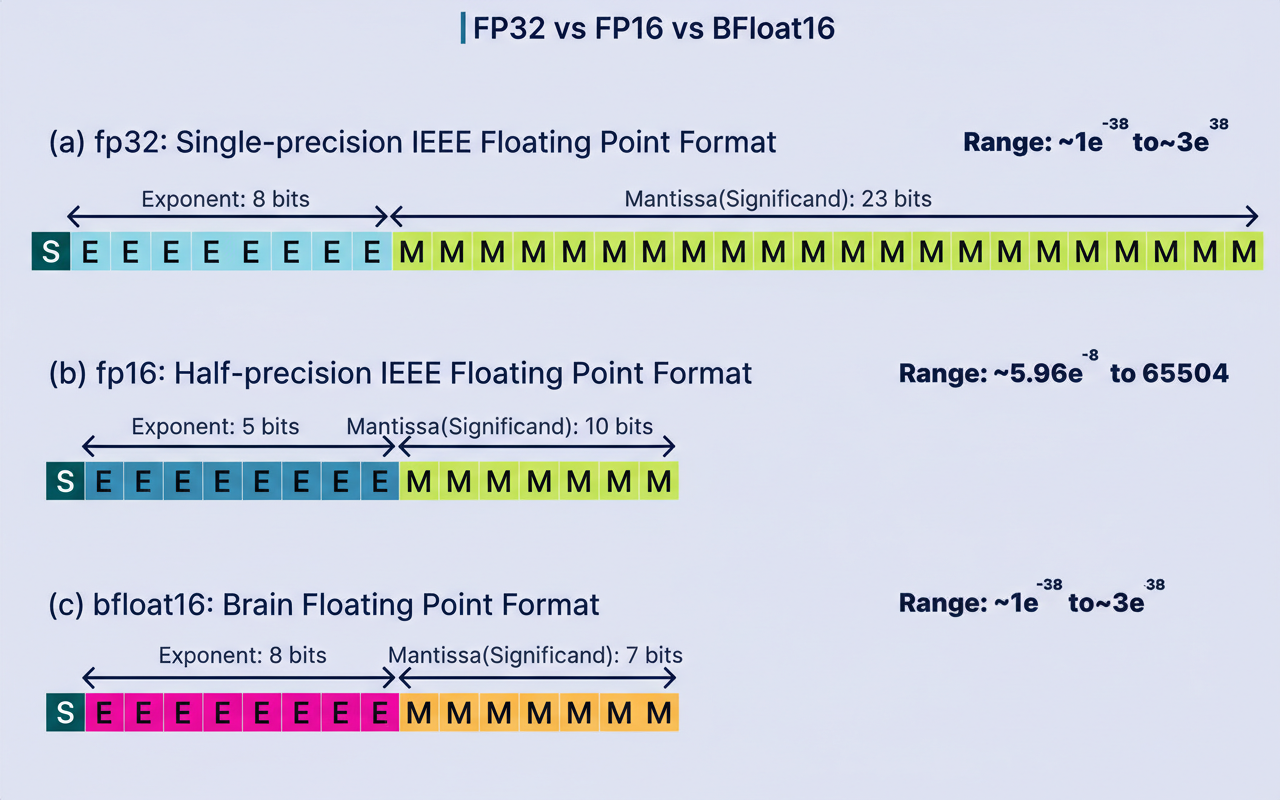
TPUs benefit from quantization, using lower-precision numeric formats than traditional floating-point arithmetic, yielding hardware efficiency advantages throughout the design. Scientific computing demands high precision to represent minute differences accurately. In contrast, neural networks calculate probabilities and patterns where exact precision is less critical.
A multiplier’s silicon area scales with the square of bit width; an 8-bit multiplier requires about 64 silicon units, whereas a 32-bit multiplier needs roughly 576 units. This explains how TPU v1 integrated 65,536 multiply-accumulate units on a modest chip, while GPUs use fewer floating-point units. More multipliers enable greater parallelism per cycle.
The first TPU utilized 8-bit integers for inference, reducing memory usage by four times compared to 32-bit floats. A 91-megabyte model shrinks to 23 megabytes with quantization. Research showed inference rarely requires 32-bit precision as extra decimal places have negligible impact on predictions.
Training requires higher precision due to incremental gradient updates over millions of iterations. Google introduced BFloat16, or Brain Floating-Point 16, for this purpose, retaining the 8-bit exponent from 32-bit floats but using only 7 bits for the mantissa. Neural networks are more sensitive to dynamic range (exponent) than precision (mantissa). BFloat16 provides wide floating-point range with half the bits, enabling efficient training without overflow issues found in alternative 16-bit formats.
Modern TPUs support multiple precision modes: BFloat16 for training, INT8 for inference running twice as fast on TPU v5e, and the newest FP8 format. Ironwood is the first TPU to support native FP8, eliminating emulation overhead present in earlier generations.
TPU development demonstrates a clear trajectory with each generation improving performance and energy efficiency, reflecting the evolving needs of AI hardware at scale.
TPU v1 debuted secretly in 2015, focused on inference. Built on 28-nanometer process technology and consuming 40 watts, it provided 92 trillion 8-bit operations per second. Connected via PCIe to standard servers, it powered Google Search, Photos, Translate, and YouTube before public knowledge. In March 2016, TPU v1 enabled AlphaGo’s victory over Lee Sedol, proving application-specific chips could outperform general-purpose GPUs by 15 to 30 times in speed and 30 to 80 times in power efficiency.
TPU v2 arrived in 2017 with architectural changes to support training, replacing the 256 by 256 8-bit array with two 128 by 128 BFloat16 arrays. It added High Bandwidth Memory (16 GB at 600 GB/s) eliminating v1’s memory bottleneck and introduced the Inter-Chip Interconnect, linking TPUs directly. TPU Pods of 256 chips operate as a single accelerator delivering 11.5 petaflops.
TPU v3 in 2018 doubled chip performance to 420 teraflops and implemented liquid cooling to manage higher power density. Pod size expanded to 1,024 chips, exceeding 100 petaflops, sufficient to train the largest models of that era efficiently.
TPU v4 in 2021 introduced SparseCores accelerating embedding operations for recommendation systems and language models by 5–7 times using only 5% of chip area. Optical Circuit Switches enabled dynamic network reconfiguration with robotic mirrors steering light beams between fibers. This allowed routing around failures and scaling to 4,096-chip Pods approaching one exaflop. The 3D torus topology connected each chip to six neighbors rather than four, reducing communication latency in distributed training.
Ironwood, or TPU v7, launched in 2025 marks the most substantial leap focused on inference deployment at scale, delivering 4,614 teraflops per chip with 192 GB HBM running at 7.4 TB/s bandwidth.
TPU deployments show substantial real-world impacts across various domains. A single TPU processes more than 100 million Google Photos daily. AlphaFold’s solution to the 50-year protein folding challenge, awarded the 2024 Nobel Prize in Chemistry, ran on TPUs. Training the 540-billion-parameter PaLM language model across 6,144 TPU v4 chips achieved 57.8% hardware utilization over 50 days, demonstrating extraordinary efficiency in distributed training.
Outside Google, TPUs power Anthropic’s Claude assistant, Midjourney’s image generation models, and numerous research breakthroughs. However, TPUs are not universally ideal. They excel at large-scale language model training and inference, convolutional neural networks, transformers with intense matrix operations, high-throughput batch processing, and workloads focused on energy efficiency. GPUs remain preferable for PyTorch-native workflows requiring the PyTorch/XLA bridge, small batch sizes, mixed AI-graphics workloads, multi-cloud deployments, and rapid prototyping.
TPUs epitomize an industry trend towards domain-specific accelerators. The general-purpose CPU model encounters physical limits when workloads escalate to trillions of operations per query. Purpose-built silicon sacrificing flexibility for efficiency delivers order-of-magnitude improvements that general-purpose optimization cannot match, essential for challenges like Shopify BFCM readiness and Black Friday Cyber Monday scale testing across global Google Cloud multi-region infrastructures handling massive edge network requests per minute.